Dual beam FIB-SEM
Helios 5 UX DualBeam
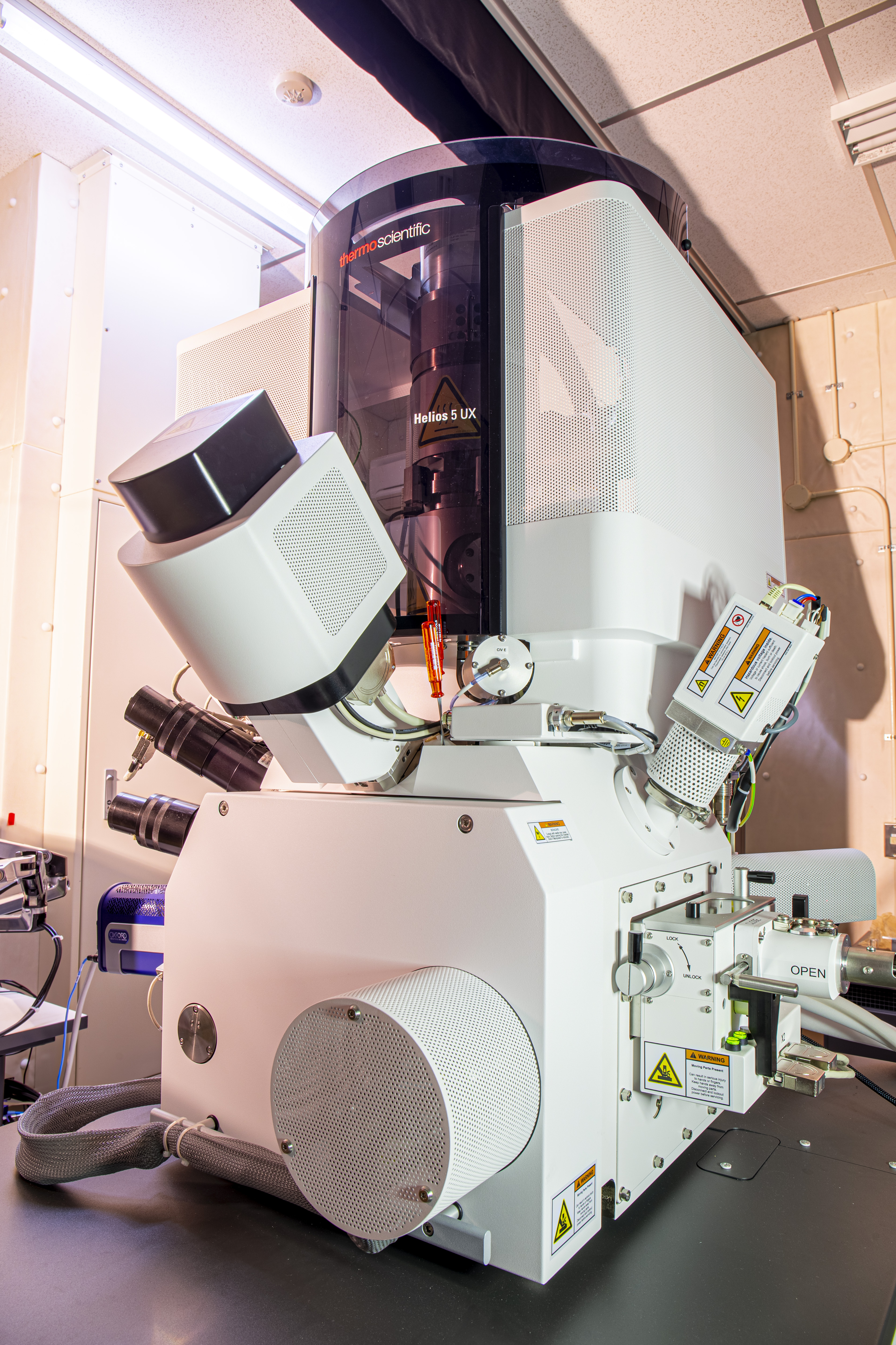 Dual Beam FIB-SEM combined with a monochromated
Field Emission SEM column and a Ga LMIS ion column. This
combination allows high-resolution SEM imaging at low
acceleration voltages during precise slicing at nanometer
orders. With the use of the fully automated TEM sample
prep system (AutoTEM5), thin lamella preparation from
lift-out to thinning and also low-kV surface cleaning will be
done automatically. The CMOS EBSD detector allows rapid
crystal orientation mapping, which is a powerful for 3D
EBSD serial sectioning.
Dual Beam FIB-SEM combined with a monochromated
Field Emission SEM column and a Ga LMIS ion column. This
combination allows high-resolution SEM imaging at low
acceleration voltages during precise slicing at nanometer
orders. With the use of the fully automated TEM sample
prep system (AutoTEM5), thin lamella preparation from
lift-out to thinning and also low-kV surface cleaning will be
done automatically. The CMOS EBSD detector allows rapid
crystal orientation mapping, which is a powerful for 3D
EBSD serial sectioning.
| SEM | Gun | Monocromated Schottky Emission |
|---|---|---|
| Acceleration Voltage | 0.35 kV - 30 kV | |
| Detectors | Through Lens SE/BSE Detector (TLD) | |
| Mirror Detector BSE (MD) | ||
| Everhart-Thornley SE Detector (ETD) | ||
| Everhart-Thornley SE検出器(ETD) | ||
| In-Chamber Secondary Electron & Ion Detector (ICE) | ||
| Directional BSE Detector (CBS/ABS) | ||
| FIB | Ion Source | Ga LMIS |
| Acc. Voltage | 0.5 - 30 kV | |
| Max. Probe Current | 65 nA | |
| FIB-SEM Geometry | V-shape (52 deg) | |
| WD | 4mm | |
| GIS | Platinum, Tungsten, Carbon | |
| Max Sample Size | 150 mm in diameter, 55 mm in height | |
| in-situ Lift-out | EasyLift | |
| Low-energy broad ion milling | - | Automation | TEM sample prep. | AutoTEM 5 |
| Serial Sectioning | Auto Slice & View 5 | |
| Montage Imaging | MAPS 3 | |
| Python Scripting | AutoScript 4 | Analysis | XEDS | - |
| EBSD | Oxford Symmetry S3 | |
| Cryo Stage | Thermo Scientific CryoMAT | |
| Air-Free Transfer | 〇 | |
| Plasma Cleaning | 〇 | |